Core8Bit build guide
This page is a step-by-step guide: from a pile of modules to a console that boots, reads the SD card, plays sound and connects to Wi-Fi. The modules and their links are in bom.md, every pin is in pinout.md, power is in power.md.
There are two build paths:
| Path | Status | What it is |
|---|---|---|
| A. Wired build | works today | the modules sit on a printed base plate and are connected with wires |
| B. Mainboard build | in development | a PCB of the same shape replaces the base plate and all the wires, see mainboard.md |
Most of this page covers path A. Path B is described briefly at the end, in Path B: building on the mainboard.
TBD marks a value that is not decided yet.
Safety. A Li-Po battery delivers high current, and a short circuit can set it on fire. Solder only with the battery disconnected. Check polarity twice. Never short 5 V to 3.3 V. Do not solder near the battery and do not heat it with a hot-air gun. Do not use a damaged or swollen battery.
Contents
- Tools and supplies
- Print the case
- Prepare the modules
- What goes where on the base plate
- Wiring by subsystem
- Mechanical assembly
- First power-on
- Troubleshooting
- Path B: building on the mainboard (in development)
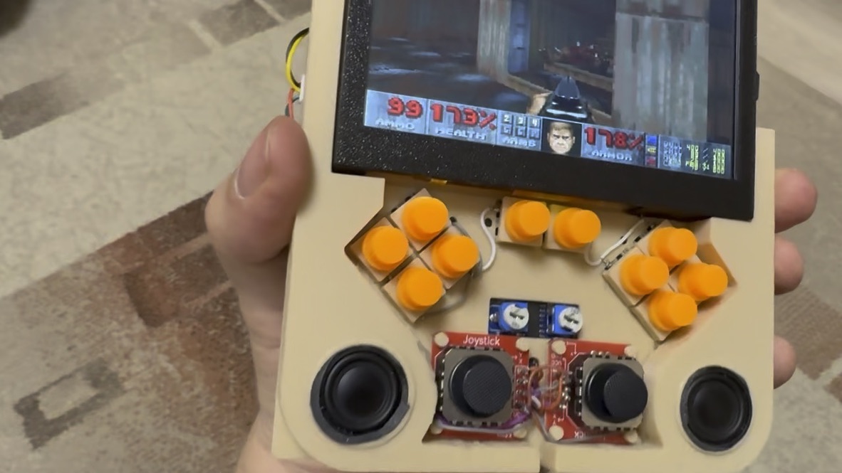
A finished wired build. At the top is the screen in a black frame. Below it: the D-pad (4 buttons) on the left, two buttons in the centre, and four buttons A/B/X/Y on the right. In the centre you can see the HW-301 (PAM8406) amplifier with its two blue volume trimmers. At the bottom are the two red stick modules and two speakers in the corners.
1. Tools and supplies
Tools
| Tool | Use |
|---|---|
| Temperature-controlled soldering iron with a fine tip (conical or mini-wave) | soldering module pins and wires to the FFC adapter contacts (0.5 mm pitch on the ribbon side, 2.54 mm pitch on the header) |
| Flux (no-clean gel), solder 0.3–0.5 mm | |
| Desoldering braid | removing bridges between neighbouring contacts |
| Multimeter with continuity tester | testing every line, measuring voltages before the first power-on |
| Bench power supply with current limit (preferred) | setting up the boosts without the battery; first power-on with a current limit |
| Tweezers, flush cutters, wire stripper | |
| Hot-glue gun | fixing the modules on the base plate posts |
| Magnifier or microscope | inspecting fine-pitch solder joints |
| ST-Link V2 or V3 | flashing the STM32 over SWD through the "SWD" connector on the core board |
| Cables: micro-USB (core board), USB-C (ESP32 DevKit) | flashing and debugging |
| 3D printer | printing the case |
| Paperclip | later, for the hard reset button on the mainboard |
Supplies
| Item | Quantity | Note |
|---|---|---|
| Hookup wire, PTFE or silicone insulated, 28–30 AWG | a few metres, several colours | signal lines |
| Wire 22–24 AWG | ~0.5 m each of red and black | power: battery, boosts, amplifier, speakers |
| 33 Ω resistors (0603/0805 or through-hole 0.125 W) | 8 + spares | series resistors on the display CLK, HSYNC, VSYNC, DE and on the ESP32 SPI lines SCK, MOSI, MISO, CS |
| Ferrite bead, ≥ 1 A (for example 600 Ω @ 100 MHz, 0805/1206 or through-hole) | 2 | in series with the 5 V output of each boost converter |
| ~10 kΩ resistor | 1 | pull-up of the ESP32 CS (GPIO5) to 3.3 V |
| ~100 kΩ resistor | 1 | pull-down of boost #1 EN to GND |
| Aluminium or copper foil tape | ~30 cm | shield for the display ribbon and adapters, connected to GND |
| Kapton or insulating tape | insulates the foil and the modules | |
| Heat-shrink tubing | ||
| Electrolytic capacitors 220 µF / 10–25 V, ceramic 100 nF | 2 each | amplifier supply filter |
| Inductor 10–47 µH rated ≥ 1 A (or a ferrite bead) | 1–2 | LC filter on the amplifier supply |
| Case screws and standoffs | see bom.md | 4 × 18 mm M3 screws, 4 × 14 mm standoffs |
| Hot glue | ||
| microSD card | 1 | see bom.md |
2. Print the case
The case has six parts. All STL files are drawn in one assembly coordinate system (mm), so you can open them together and see the assembled console. The Z axis points to the front: the front surface of the case is at Z = +2, the back at Z = −22. The console is about 24 mm thick overall.
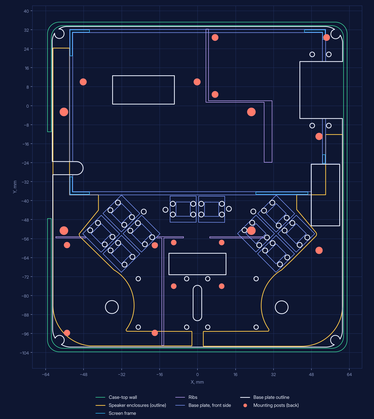
Layer by layer: base plate outline (white), front-side features of the base plate (blue), mounting posts on the back (red dots), ribs (magenta), case-top wall (green), screen frame (cyan), speaker enclosures shown as outlines only (orange). Coordinates in mm, assembly coordinate system.
Download: case files (zip, 1.7 MB), or one by one below. Free for your own build: one click to accept the agreement before the first download. Selling consoles you build? Read the rules. The speaker enclosures spk-L and spk-R are sold separately on our itch.io page.
| File | Part | Overall size, mm | What it has |
|---|---|---|---|
case-top.stl |
case front | 126.3 × 138.9 × 22.5 | 1.5 mm front wall with the screen window and holes for the buttons and sticks; side walls; 4 corner tubes (inner diameter about 5 mm) for the standoffs |
case-back.stl |
back cover | 126.2 × 138.9 × 5 | wall about 1.6 mm; 4 corner holes of about 3.5 mm with a counterbore of about 6.2 mm for the screw head; ribs up to Z = −17 that support the base plate |
base-plate.stl |
base plate | 122.3 × 135.1, 1.5 thick (7.5 with posts) | buttons and sticks on the front side; locating posts on the back that fit the module holes |
screen-frame.stl |
screen frame | 110.6 × 70.5 × 11.5 | holds the cover glass, the display, and the battery behind it |
spk-L.stl (itch.io) |
left speaker enclosure | 58.6 × 125.5 × 10 | acoustic labyrinth along the left edge and a seat for a 20 mm speaker |
spk-R.stl (itch.io) |
right speaker enclosure | 58.7 × 89.2 × 10 | the same on the right |
Internal cavities: at the front, about 10 mm between the base plate and the front wall (buttons, sticks, speaker labyrinths); at the back, about 9.4 mm between the base plate and the back cover (modules on the back).
Print settings
| Parameter | Setting | Why |
|---|---|---|
| Material | PETG (or PLA for a test build; ABS/ASA if you have an enclosed printer) | PETG is stronger and handles heat from the battery and the boosts better than PLA |
| Nozzle / layer | 0.4 mm / 0.2 mm; 0.12–0.16 mm is fine for case-top and screen-frame |
thin front parts |
| Perimeters | 3 (wall at least 1.2 mm) | the screw tubes and posts need solid walls |
| Infill | 20–30 %, gyroid; 40 % for base-plate |
the base plate carries all the modules and must not bend |
| Solid top/bottom layers | 4–5 | the front wall is only 1.5 mm and must be solid |
case-top orientation |
front side down on the bed | smooth front surface; the corner tubes grow upward without supports |
case-back orientation |
outer side down on the bed | the screw-head counterbores come out clean |
base-plate orientation |
front side down, posts up | the posts print without supports; the front side stays flat (the buttons sit on it) |
screen-frame orientation |
front side down on the bed | the inner steps for the glass and the display face up; no supports needed |
spk-L / spk-R orientation |
bottom (Z = −9) on the bed | the labyrinth lid (about 0.75 mm) prints as bridges over the channels |
| Supports | not needed for any part in these orientations (check the slicer preview) | |
| Brim | 3–5 mm for case-top and case-back |
large flat parts; PETG can lift at the corners |
Warning:
spk-L.stlis not watertight. If the slicer complains, enable model repair, or run it through Meshmixer or PrusaSlicer "Fix through Netfabb". The labyrinth must stay airtight, or the bass is lost.
After printing:
- Remove the brim. Clean up burrs in the button holes.
- Clear the Ø 2.1 mm holes for the button legs and the Ø 1.85 mm holes for the stick mounting with a drill or a needle if they are partly closed.
- Test-fit all parts without electronics. The base plate must sit on the ribs of the back cover, and the screen frame must fit into the window of the case front.
3. Prepare the modules
Prepare and test each module separately, before you install it in the case. A fault is ten times easier to find on the bench than inside an assembled console.
3.1. STM32H7 core board
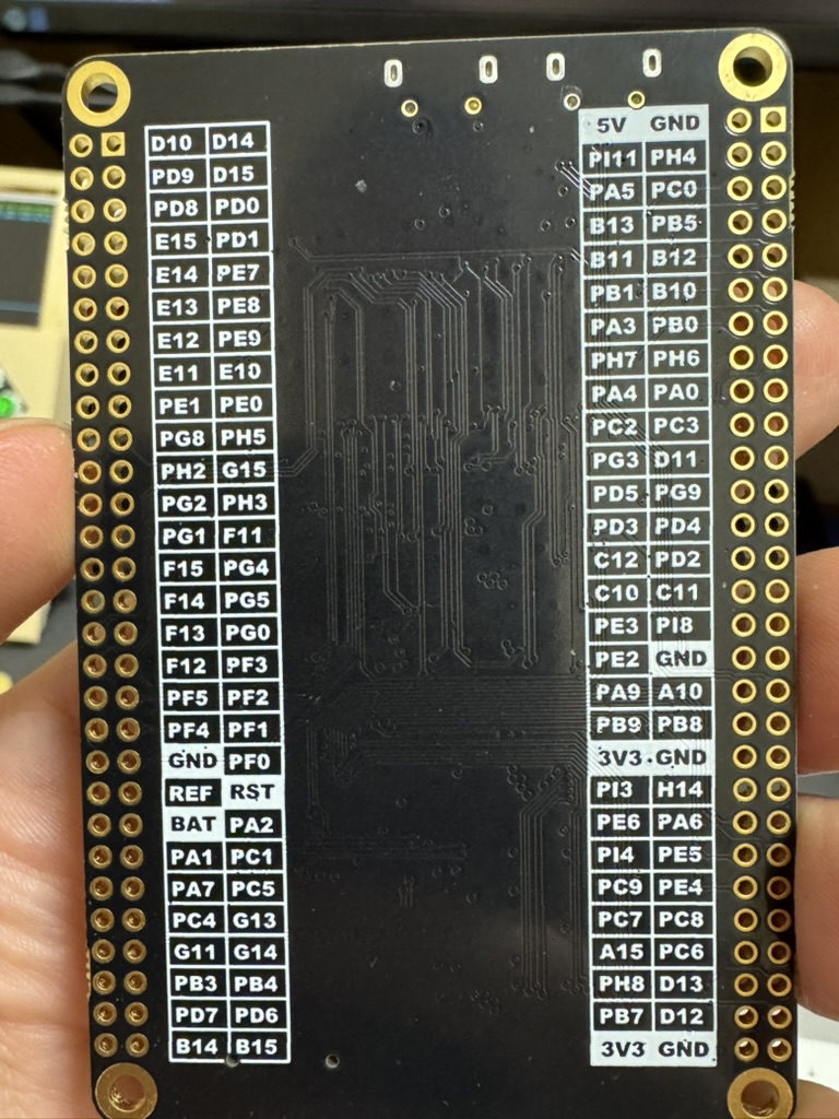
- Read the chip marking. The firmware is built for the STM32H753IIT6 in LQFP176 (176 pins; an H743IIT6 in the same package also works). The "VIT6" version (LQFP100) does not work: it has no ports H and I. See hardware.md.
- Check that the board has a 25 MHz HSE crystal, a 32.768 kHz LSE crystal, Winbond SDRAM and a microSD slot.
- Connect the ST-Link to the "SWD" connector (SWDIO, SWCLK, GND, 3.3 V; NRST if possible). Power the core board from USB and connect nothing else.
- Check the connection:
STM32_Programmer_CLI -c port=SWD. If the board is stuck in a crash loop, connect under reset:STM32_Programmer_CLI -c port=SWD mode=UR.
3.2. Flash the STM32 (BIOS)
Download Core8Bit.elf from the firmware release and flash it over SWD:
STM32_Programmer_CLI -c port=SWD -w Core8Bit.elf -v -rst
You can flash the BIOS right away, before assembly: the board starts even without a display.
3.3. Flash the ESP32
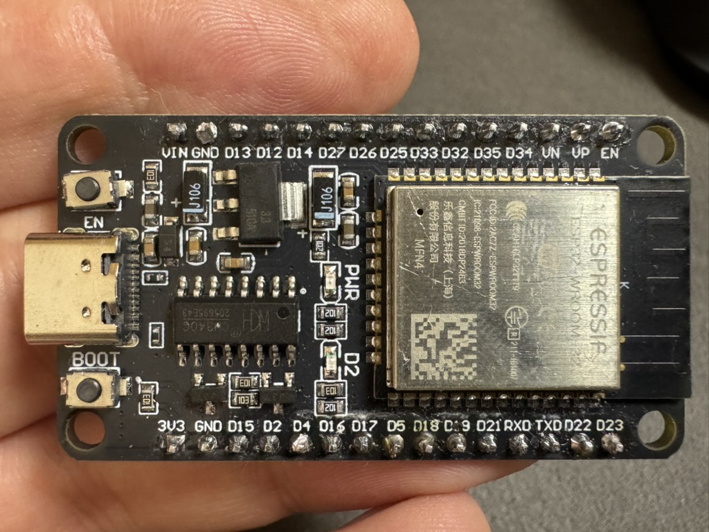
You need a classic ESP32 (not S2/S3/C3), module ESP32-WROOM-32.
Download the ESP32 Wi-Fi firmware from the firmware release and flash it over the DevKit USB-UART with the flash command given in the release notes. Then open a serial monitor at 115200 baud: it must print a line like === SPI Slave v4 Init ... MOSI=23 MISO=19 SCLK=18 CS=5 DRDY=4 .... Flash the ESP32 before you install it in the case: later the DevKit USB-C is covered.
Do not connect the ESP32 USB while the console's 5 V rail is on, unless VIN has a diode: two 5 V sources will fight each other. Flash the ESP32 with the console switched off.
3.4. Boost #1 and #2 (5 V)
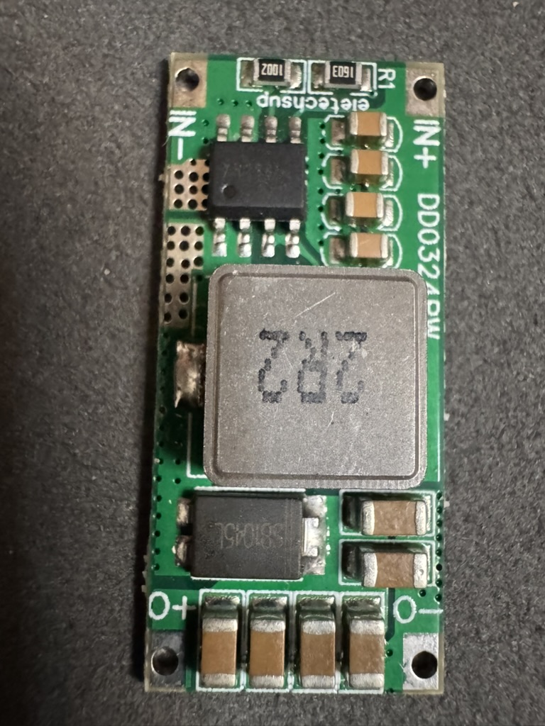
Both boosts are identical step-up modules. Roles:
- Boost #2: permanent supply of the STM32 core board (always on). Its EN is not used for hard reset (see the note below); the mainboard resets the STM32 through NRST instead, see mainboard.md.
- Boost #1: the switched 5 V rail for the ESP32, the PAM8406 amplifier and the 21 V backlight booster. It is enabled by PE4 (HIGH = rail on, LOW = rail off).
Setup:
- Apply 3.7 V to
IN+/IN−from a bench supply (0.5 A current limit) or from a charged battery through the charger board. - Measure
O+/O−with no load. You need 5.0–5.1 V. - This module has no trimmer: a feedback divider (the resistors near the
R1mark) sets the output voltage. If you bought a version with a trimmer, set it to 5.0–5.1 V. If a fixed module is out of range, replace it; reworking the divider is not recommended. - Load the output with a 10–20 Ω resistor (250–500 mA) for a few seconds. The voltage must not drop below 4.9 V.
- Label the modules with a marker: "#1 PE4" and "#2 STM32".
EN pin. The module has no labelled EN pad. Use the EN/SHDN pin of the SO-8 controller; find it in the datasheet of the controller on your module. See power.md.
- For boost #1, connect EN to PE4 (header R24.2). Fit a 100 kΩ pull-down from EN to GND, so the rail stays off while the STM32 is in reset.
- Boost #2 EN stays as on the module (always on). It is not wired to a reset button.
Note. With a plain asynchronous boost, EN = LOW does not bring the output to zero: the battery voltage passes to the output through the inductor and the diode (about VBAT − 0.3 V). Measure the output with EN = GND. If you see 3.4–3.9 V, the "off" 5 V rail actually feeds the ESP32 and the amplifier with battery voltage. For a full cut-off you need a boost with true load disconnect or a P-MOSFET switch on the output.
3.5. 21 V backlight booster
The HL043PQIPS-500 backlight: 8 LEDs in series, 21 V / 40 mA (pin 2 LEDA = anode, pin 1 LEDK = cathode). The booster runs from boost #1 (the PE4 rail), so the backlight turns on and off together with PE4. Brightness is not PWM-controlled.
Setup:
- If the module has a voltage trimmer: with no load, set it to about 19 V, never above 21 V.
- Connect the panel backlight through a milliammeter in series with LEDA.
- Raise the voltage slowly until the current is about 30–40 mA. Do not exceed 40 mA: the backlight LEDs overheat and degrade.
- If the module regulates current (an LED driver), check that its current is no more than 40 mA.
3.6. PAM8406 amplifier (HW-301)
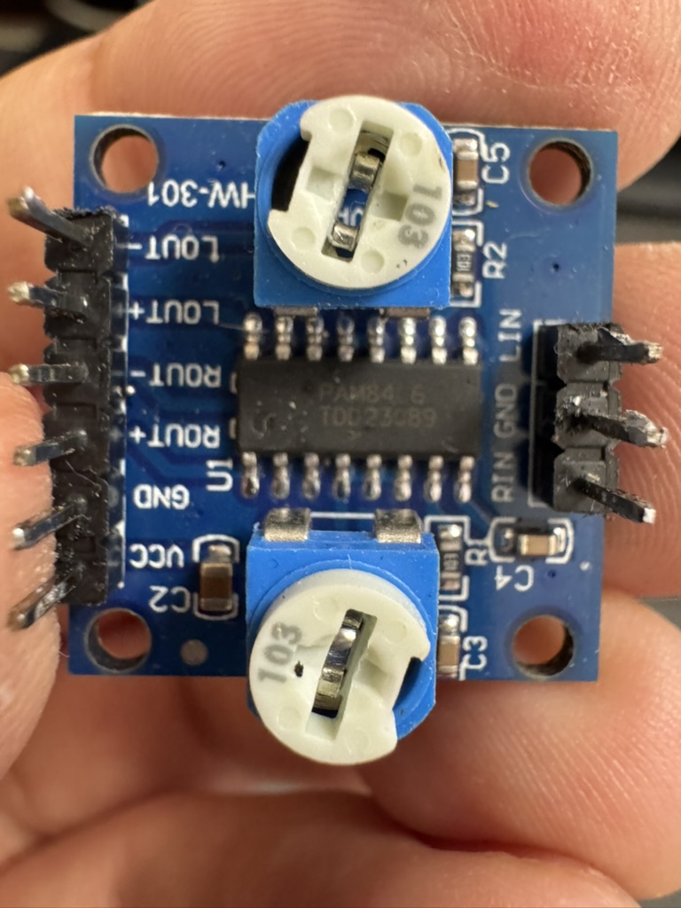
Contacts: output and power LOUT− LOUT+ ROUT− ROUT+ GND VCC, input LIN GND RIN.
- The two
103(10 kΩ) trimmers set the volume of the left and right channels. - Before the first power-on, set both trimmers to about one third of their travel. Full volume with small 20 mm speakers causes rasping and overload.
- Set the final volume after assembly: play music at maximum BIOS volume (MENU+RIGHT) and turn the trimmer up until the sound starts to distort, then back it off a little.
- The outputs are bridge-tied: never connect
LOUT−/ROUT−to GND or to each other.
3.7. Sticks and buttons
- Sticks (red "Joystick" modules): each axis has its own potentiometer between 3.3 V and GND, with the wiper on an ADC input. Check with a multimeter that the wiper resistance changes smoothly over the full travel. Power the sticks from 3.3 V only, never from 5 V: the STM32 ADC inputs are rated for 3.3 V.
- Buttons (10 identical): find out with the continuity tester which pairs of legs close when pressed. On 4-leg tactile buttons, two pairs of legs are always connected inside.
3.8. FFC adapters and ribbon
Two 40-pin adapters (0.5 mm pitch) and a 40-pin 6 cm ribbon. One adapter sits at the screen, the other at the core board's "LCD interface" connector. The folded layout is described in 5.1. Display.
3.9. SD card
- Format the card as FAT32 (exFAT is also supported), one partition.
- Copy the SD card contents from the firmware release:
0:/System/     launcher/, sdk/ (system Lua bindings), fonts/, assets/, joystick_cal.dat
0:/Games/      one folder per game (main.lua, icon.stj, plugins/*.bin, data)
0:/fw-assets/  core8bit.c8sf  -> flashed into QSPI at boot
- On a new build, delete
System/joystick_cal.dat: it holds a calibration from another unit. You will make your own calibration at the first power-on. - Put the sound bank
core8bit.c8sfin0:/fw-assets/. At boot the BIOS checks it, writes it to QSPI at address 0x90010000, shows progress and deletes the file from the card. The file is part of the firmware release.
4. What goes where on the base plate
Coordinates: front view, X to the right, Y up, mm, assembly coordinate system. On the back (rear view) everything is mirrored in X. Test-fit each module on its posts before gluing.
Front side
| What | Where | Mounting |
|---|---|---|
| Screen frame with display and battery | top of the plate, area about X −55…55, Y −38…32 | the frame rests on the plate and is held down by the case front |
| D-pad (4 buttons, rotated 45°) | left, about X −45…−19, Y −41…−67 | legs in Ø 2.1 mm holes |
| Two centre buttons | centre, about X −10…10, Y −41…−46 | legs in Ø 2.1 mm holes; MENU and SELECT |
| A / B / X / Y (4 buttons, rotated 45°) | right, about X 20…46, Y −41…−67 | legs in Ø 2.1 mm holes |
| Amplifier window (trimmers) | centre, 24 × 9 mm cut-out at Y ≈ −66.6 | amplifier board on 4 posts (20.2 × 18.4 mm) at about X ±10, Y −58…−76 |
| Left and right sticks | bottom centre, 4 holes Ø 1.85 mm each at 20.4 × 20.4 mm pitch (X −25…−4.6 and 4.3…24.7, Y −73…−93) | screws or posts; wires through the 3.6 × 15 mm slot between the sticks |
Speaker enclosures spk-L/spk-R with labyrinths |
along the left and right edges and in the bottom corners | held down by the case front |
| Speaker wire holes | Ø 5.5 mm at about X ±36, Y −85 |
Back side (modules)
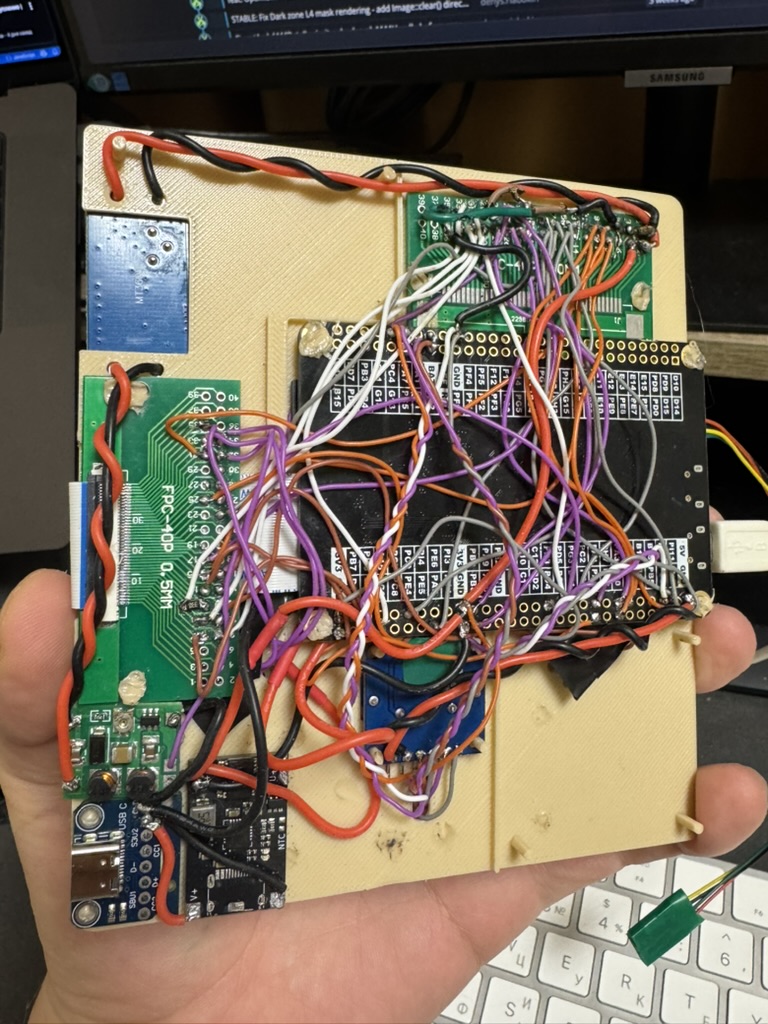
Back of the base plate (rear view, so mirrored). In the centre is the STM32H7 core board (the header silkscreen is visible). On the left is the vertical green FFC adapter "FPC-40P 0.5MM"; the second adapter is at the top right. At the top left is a blue module in a cut-out of the plate. At the bottom left are the power modules: a green board, a blue USB-C breakout board (contacts CC1, CC2, D+, D−, SBU, VBUS) and a black board. At the bottom centre is a blue module with twisted wires. The modules sit on beige posts and are fixed with hot glue.
| Posts (front view), mm | Spacing | For |
|---|---|---|
| X −56.3 / 22.7, Y −2.65 / −52.65, Ø 3.4 | 79 × 50 | STM32H7 core board |
| X 7.4 / 54.4, Y 28.7 and X 7.4, Y 4.7, Ø 2.6 | 47 × 24 (three posts) | ESP32 DevKit |
| X −48.2 / −0.2, Y 10, Ø 2.7 | 48 | horizontal FFC adapter |
| X 51.2, Y −13 / −61, Ø 2.8 | 48 | vertical FFC adapter |
| X −10 / 10.2, Y −57.7 / −76.1, Ø 2.1 | 20.2 × 18.4 | PAM8406 amplifier |
| X −55 / −18, Y −58.7 / −95.7, Ø 2.4 | 37 × 37 | free area (VS1003B on the mainboard) |
| Ø 2.0 mm holes: X 48.3 / 55.3, Y −8.4 / 21.6 | 7 × 30 | module at the plate cut-out (blue board, top left) |
Other through slots: 26 × 12 mm at about X −22.8, Y 6.7, and 12 × 26 mm at about X 53.8, Y −37.6. They pass the battery wires and the screen ribbon from the front side to the back.
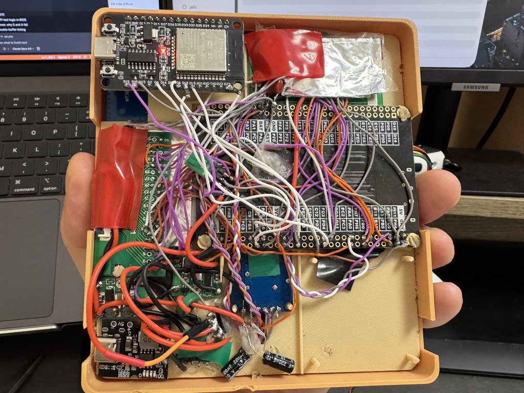
The same assembly placed in the orange back part of the case. At the top left is the ESP32 DevKit (USB-C at the left edge). At the top right the FFC adapter is covered with aluminium foil (shield), with red electrical tape next to it. On the left, the vertical adapter is under red electrical tape. At the bottom left are the power modules, at the bottom two 220 µF electrolytics, and at the bottom centre the blue module with twisted wire pairs.
5. Wiring by subsystem
General rules:
- Keep the battery disconnected the whole time you solder.
- First place the modules on the posts (no glue), run the wires and test them. Only then fix everything with hot glue.
- Keep signal wires as short as the routing allows. Keep the lines of one bus (display RGB, SPI) about the same length.
- Star ground: all GND wires meet at one point near the charger board output / boost inputs, see 5.7.
- Location names on the core board:
R12.1= right header block, position 12, row 1 (from the back silkscreen).FPCn= contact n of the "LCD interface" connector. Full tables are in pinout.md. Ring out once which physical row of holes is "row 1".
5.1. Display
First read pinout.md → Display ribbon (40-pin, folded) and Panel FPC pinout.
The chain:
 display FPC ──► adapter at screen ──► 40-pin ribbon ──► adapter at board ──► core board "LCD interface"
 (pin n)         (fold #1, mirror)      (wire k)          (fold #2, mirror)    (pin m = 41 − k)
                  contact = 41 − n                                             + wires from the headers
Mirroring trap. Under each adapter the ribbon is folded in half, and each fold reverses the contact order: pin n becomes 41 − n. Board-side adapter pad numbers are not panel pins. For example, VSYNC is on pad 32, but the panel needs it on pin 33; DE is on pad 33, but the panel's DEN pin is 34. Therefore:
- Find and mark pin 1 on both adapters and on the display FPC (from the silkscreen and the datasheet) before you solder.
- Solder by function (VSYNC to VSYNC), not by number.
- If you run the ribbon without a fold, the numbers change. All numbers below assume a fold under each adapter.
Steps:
- Insert the ribbon into the core board's "LCD interface" connector, fold it under the board-side adapter and insert it into the adapter.
- Insert the display FPC into the screen-side adapter the same way, with a fold. Adapter contact = 41 − panel pin.
- Take the lines that exist only on the "LCD interface" connector (CLK, VSYNC, DE, R4, R7, G5, B3, B4) from the contacts of the board-side adapter. The others (HSYNC, DISP, R3, R5, R6, G2, G3, G4, G6, G7, B5, B6, B7) come as wires from the core board headers.
- Run every line to the contacts of the screen-side adapter by function, using the table below.
- Solder 33 Ω series resistors into CLK, HSYNC, VSYNC and DE. Place them at the STM32 end (at the board-side adapter or the header), not at the screen. This damps edge ringing.
- Leave contact 40 of the board-side adapter unconnected: it is pin 1 of the board connector = PE2 = the SPI4 clock to the ESP32.
- The panel's low colour bits (R0–R2, G0–G1, B0–B2) are not used: the firmware runs RGB565 on the high bits. Tie them to GND. Leave PA10 (B1) unconnected.
- Connect the backlight (pins 1 LEDK and 2 LEDA) to the 21 V booster output (see 3.5).
- Panel logic supply: pin 4 VCC ← 3.3 V (header R20.1 or R29.1); pins 3, 29, 36 GND ← GND.
| Panel pin | Signal | From STM32 | Where on the core board | Screen-side adapter contact (41 − n) | Resistor |
|---|---|---|---|---|---|
| 1 | LEDK | — | 21 V booster minus | 40 | |
| 2 | LEDA | — | 21 V booster plus | 39 | |
| 3, 29, 36 | GND | — | GND | 38, 12, 5 | |
| 4 | VCC 3.3 V | — | R20.1 / R29.1, or board-side adapter contact 11 (FPC30 = 3V3) | 37 | |
| 8 | R3 | PB0 | R7.2 | 33 | |
| 9 | R4 | PH15 | board-side adapter contact 16 (FPC25) | 32 | |
| 10 | R5 | PC0 | R3.2 | 31 | |
| 11 | R6 | PB1 | R6.1 | 30 | |
| 12 | R7 | PG6 | board-side adapter contact 10 (FPC31) | 29 | |
| 15 | G2 | PA6 | R22.2 | 26 | |
| 16 | G3 | PC9 | R24.1 | 25 | |
| 17 | G4 | PH4 | R2.2 | 24 | |
| 18 | G5 | PI0 | board-side adapter contact 17 (FPC24) | 23 | |
| 19 | G6 | PI11 | R2.1 | 22 | |
| 20 | G7 | PD3 | R13.1 | 21 | |
| 24 | B3 | PA8 | board-side adapter contact 24 (FPC17) | 17 | |
| 25 | B4 | PG12 | board-side adapter contact 25 (FPC16) | 16 | |
| 26 | B5 | PA3 | R7.1 | 15 | |
| 27 | B6 | PB8 | R19.2 | 14 | |
| 28 | B7 | PB9 | R19.1 | 13 | |
| 30 | CLK | PG7 | board-side adapter contact 30 (FPC11) | 11 | 33 Ω |
| 31 | DISP | PD5 (called "DEN" in the firmware, GPIO, HIGH = on) | R12.1 | 10 | |
| 32 | HSYNC | PC6 | R26.2 | 9 | 33 Ω |
| 33 | VSYNC | PI9 | board-side adapter contact 32 (FPC9) | 8 | 33 Ω |
| 34 | DEN (data enable) | PF10 (LTDC_DE) | board-side adapter contact 33 (FPC8) | 7 | 33 Ω |
| 5–7, 13–14, 21–23 | R0–R2, G0–G1, B0–B2 | not used | — | 36–34, 28–27, 20–18 | to GND |
| 35, 37–40 | NC, resistive touch | — | do not connect | 6, 4–1 |
Before you power on, ring out every line (the 3 steps in pinout.md): put one probe on the STM32 signal, move the other along the panel FPC contacts until it beeps, and compare with the table.
Shielding. Wrap the ribbon and both adapters in foil tape. Insulate the contacts with Kapton first, then connect the foil to GND at one point. Without a shield the picture jitters and drifts. Keep the foil away from the ESP32 antenna.
5.2. Buttons
All buttons are active HIGH: a press connects the pin to 3.3 V, and the internal pull-down holds it LOW when released. Do not connect the buttons to GND, or they will read as "always pressed".
| Button | STM32 pin | Where to solder |
|---|---|---|
| UP | PI10 | board-side adapter contact 31 (FPC10) |
| DOWN | PI6 | contact 27 (FPC14) |
| LEFT | PI7 | contact 28 (FPC13) |
| RIGHT | PH6 | header R8.2 or contact 34 (FPC7) |
| A | PH9 | contact 6 (FPC35) |
| B | PH10 | contact 7 (FPC34) |
| X | PH11 | contact 8 (FPC33) |
| Y | PH12 | contact 9 (FPC32) |
| MENU | PA0 | header R9.2 |
| SELECT | PI5 | contact 26 (FPC15) |
| common 3.3 V | — | adapter contact 11 (FPC30 = 3V3) or header R20.1 / R29.1 |
Run one common 3.3 V bus along the front side and one signal wire from each button through the base plate to the back.
Roles: MENU is the combo modifier (MENU+A console, MENU+B exit game, MENU+UP Wi-Fi, MENU+DOWN sleep, MENU+LEFT/RIGHT volume) and the wake-up button. SELECT opens the system menu.
5.3. Sticks
| Axis | Wiper → STM32 pin | Header position | Potentiometer ends |
|---|---|---|---|
| Right X | PA2 | L22.2 | 3.3 V / GND |
| Right Y | PA7 | L24.1 | 3.3 V / GND |
| Left X | PC1 | L23.2 | 3.3 V / GND |
| Left Y | PC4 | L25.1 | 3.3 V / GND |
Axis direction does not matter: the calibration wizard detects inverted axes by itself. Do not swap the right and left sticks: PA2/PA7 is the right stick, PC1/PC4 the left. The firmware does not read the stick click buttons. The stick wires pass to the back through the slot between the sticks.
5.4. SD card
The microSD slot is already on the core board (SDMMC2, 4-bit); there is nothing to solder. The SD lines are also brought out to the header (L27–L29: PB3, PB4, PD7, PD6, PB14, PB15). Connect nothing to them, or the card will stop mounting. Keep access to the slot through the case, or insert the card before you close the case.
5.5. ESP32 (SPI4)
Seven wires:
| # | Signal | STM32 | Header position | ESP32 DevKit | Suggested colour |
|---|---|---|---|---|---|
| 1 | GND | GND | R17.2 | GND | black |
| 2 | +5 V | boost #1 output (PE4 rail) | — | VIN | red |
| 3 | SCK | PE2 | R17.1 | D18 | yellow |
| 4 | MOSI | PE6 | R22.1 | D23 | green |
| 5 | MISO | PE5 | R23.2 | D19 | blue |
| 6 | CS | PD2 | R14.2 | D5 | orange |
| 7 | DRDY | PD4 | R13.2 | D4 | white |
-
Fit a ~10 kΩ pull-up to 3.3 V on D5 (GPIO5). GPIO5 is an ESP32 strapping pin: if CS is LOW while the ESP32 boots, it does not start.
-
Solder a 33 Ω resistor in series into each SPI data line, at the end that drives it:
Line Resistor at SCK, MOSI, CS the STM32 end (header) MISO the ESP32 end (D19) Without them the fast edges ring on the wires and the link drops packets or loses sync.
-
Keep the SPI wires short and equal in length (the link runs at 7.5 MHz). Run them as a bundle along the top edge.
-
Keep the ESP32 antenna (the module edge with the zigzag) away from the battery, the foil and the power wires.
5.6. Power: battery, charger, boosts, PE4
USB (charge) ─► charger board ◄─► Li-Po 606090 1S
                   │ OUT+
                   ├─► boost #2 (always on) ─► FB ─► 5 V ─► core board (5 V input: TBD) ─► on-board 3.3 V
                   └─► boost #1 (EN ◄─ PE4, R24.2) ─► FB ─► 5 V sw ─┬─► ESP32 VIN
                                                                   ├─► PAM8406 VCC (through LC filter)
                                                                   └─► 21 V booster ─► backlight
| From | To | Wire | Note |
|---|---|---|---|
| Li-Po + / − | charger board battery contacts | 22–24 AWG | check polarity twice |
| charger board OUT+ / OUT− | IN+ / IN− of boost #1 and boost #2 | 22–24 AWG | run from one point (star) |
| boost #2 O+ / O− | core board 5 V input / GND | 22–24 AWG | through a ferrite bead in the + line, right at the module; header pin 5V (R1.1) or the board's USB jack: TBD |
| PE4 (R24.2) | boost #1 EN | signal | + 100 kΩ pull-down to GND |
| boost #1 O+ / O− | ESP32 VIN/GND, PAM8406 VCC/GND, 21 V booster input | 22–24 AWG | through a ferrite bead in the + line, right at the module, before the line splits |
core board BAT (L22.1) |
? | this is the MCU VBAT input; the BIOS measures the battery on it. The pin limit is 3.6 V; a full battery is 4.2 V, so never connect the cell straight to it. The circuit in between is TBD, see power.md |
How PE4 works: right after reset the firmware holds PE4 LOW. During the cold-boot charge check the rail stays off. Then the DAC ramps smoothly to mid-scale, and only then PE4 goes HIGH, so the amplifier does not pop. Details: power.md.
Firmware discharge threshold: 3050 mV (0 % and automatic sleep). Cold boot only from 10 %.
5.7. Sound: DAC → amplifier → speakers
| From | To | Note |
|---|---|---|
| PA4 (DAC1_OUT1, R9.1) | LIN |
left channel |
| PA5 (DAC1_OUT2, R3.1) | RIN |
right channel |
| core board GND (next to PA4/PA5) | input GND |
separate wire, twisted with the signal wires |
| boost #1 through the LC filter | VCC / power GND |
see below |
LOUT+ / LOUT− |
left speaker | bridge-tied output, LOUT− not to GND |
ROUT+ / ROUT− |
right speaker | the same |
Against hiss and noise:
- Twisted pairs. Twist each signal with its ground from the DAC to the amplifier input. Twist the wires to each speaker in pairs too.
- Short wires at the amplifier input: place the amplifier near the header and keep the PA4/PA5 wires no longer than 5–7 cm.
- LC filter on the amplifier supply: a 10–47 µH inductor (≥ 1 A) in series with
VCC, followed by a 220 µF electrolytic + 100 nF ceramic right at the amplifierVCC/GNDcontacts. - RC filter on the DAC output (optional): 1 kΩ in series + 10 nF to GND at the amplifier input, cut-off about 16 kHz. The DAC runs at 22 050 Hz; the filter removes the steps.
- Star ground: run the amplifier power ground straight to the common GND point of the boosts, and the input ground to the core board GND. Do not route speaker current through the core board ground.
- Keep the speaker wires and the amplifier away from the display ribbon and the boosts.
5.8. USB
On the wired build, USB goes through the "USB" micro-USB jack on the core board (SD card mode for a PC and the debug CDC). An external USB-C with OTG and a single charging point is planned for the mainboard, see mainboard.md.
The firmware currently works only as a USB device. If you fit an external USB-C, do not put 56 kΩ resistors on CC (they announce the port as a host) on a port that connects to a PC. Details: mainboard.md.
6. Mechanical assembly
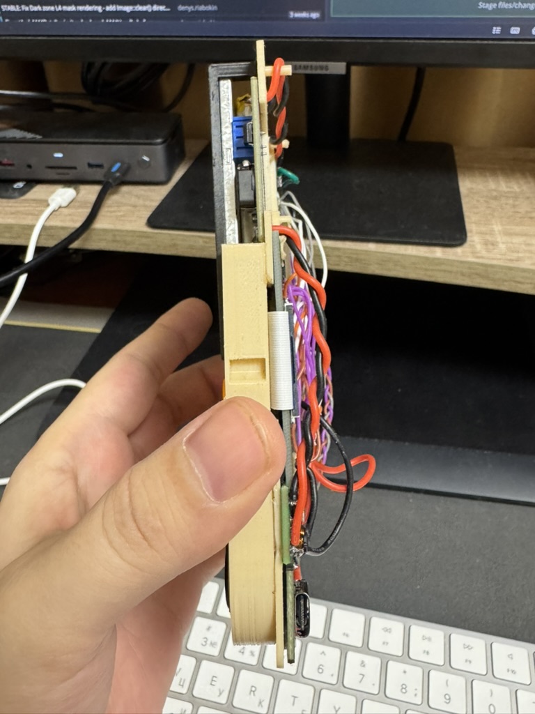
Side view: the front (left in the photo) is the screen frame, with the base plate and the wiring on its back below it. At the bottom is the thick beige part, the speaker enclosure with the labyrinth. The USB-C connector is visible at the bottom right.
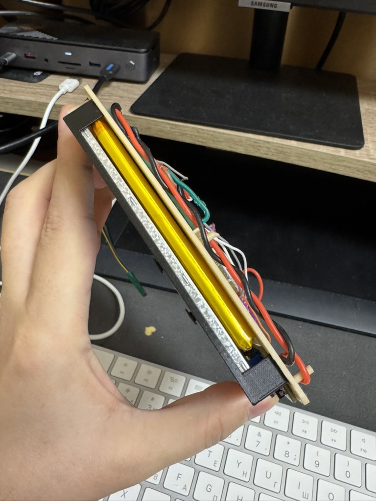
The battery (yellow 606090 pouch) sits behind the display, between the back of the display and the base plate, inside the screen frame.
Order:
- Glass and screen into the frame. Place
screen-frameface down on a soft cloth. Clean the cover glass and put it into the top step of the frame. Put the HL043PQIPS-500 display on top, face towards the glass. There must be no dust between them; use sticky tape to pick up specks. Route the display FPC towards the screen-side adapter. - Battery behind the display. Place the 606090 battery on the back of the display (inside the same frame). Put a layer of Kapton or thin foam tape between the battery and the display. Do not press on the display and do not put sharp objects on the battery. Route the battery wires through the slot to the back of the base plate.
- Buttons and sticks on the front of the base plate. Insert the button legs into the Ø 2.1 mm holes and mount the sticks on the Ø 1.85 mm holes. Check that the buttons sit level (under the rubber caps from the BOM).
- Modules on the back. Place the core board, the ESP32, the adapters, the amplifier and the power modules on the posts. No glue yet.
- Wiring as in section 5. Test every line. Then fix the modules and wire bundles with drops of hot glue on the posts.
- Speakers into the speaker enclosures. Insert the 20 mm speakers into the seats of
spk-L/spk-Rtightly, with no gaps: the labyrinth works only if no air leaks past the cone. If a seat is loose, wrap the speaker rim with thin foam tape or run a ring of hot glue around the edge (not on the cone). Route the speaker wires through the Ø 5.5 mm holes in the base plate. - Speaker enclosures into the case front. The speaker enclosures go into the pockets of
case-topalong the edges and in the bottom corners. Press them firmly against the front wall. - Base plate into the case front. Insert the button caps into the holes of
case-top. Placecase-topface down, put the screen frame with the display and battery into the window, then the base plate front side down. Make sure no wires are trapped between the plate and the walls. - First power-on before closing the case: section 7.
- Closing. Fit the back cover
case-back: its ribs rest on the base plate. Drive in the 4 corner screws.
Put the 14 mm standoffs into the 4 corner tubes of case-top (inner diameter about 5 mm). Pass the 18 mm M3 screws through the corner holes of case-back (about 3.5 mm, with a 6.2 mm counterbore for the head) into the standoffs. The base plate's semicircular corner cut-outs clear the tubes.
11. Do not overtighten the screws: the plastic tubes will crack.
7. First power-on
7.1. Voltages before connecting the STM32
While the core board is not connected to power (remove the wire from boost #2 to the core board):
| # | What to measure | Where | Expected | If not |
|---|---|---|---|---|
| 1 | Battery | charger board battery contacts | 3.0–4.2 V | the battery is flat or its protection has cut it off: put it on charge |
| 2 | Charger board output | OUT+ / OUT− | ≈ battery voltage | faulty charger board or wiring |
| 3 | Boost #2, no load | O+ / O− | 5.0–5.1 V | see 3.4 |
| 4 | Boost #1, EN to GND | O+ / O− | about 0 V, or VBAT − 0.3 V on a boost without load disconnect (see the warning in 3.4) | if 5 V: EN does not work, check the EN wire |
| 5 | Boost #1, EN temporarily to 3.3 V | O+ / O− | 5.0–5.1 V | |
| 6 | 21 V booster (backlight disconnected) | output | no more than 21 V | see 3.5 |
| 7 | No short on the 3.3 V rail | core board 3V3 ↔ GND (power off, resistance mode) | not zero (usually hundreds of ohms or more) | look for a solder bridge |
| 8 | No short 5 V ↔ 3.3 V | boost O+ ↔ 3V3 | open circuit | look for a wiring error |
Then reconnect boost #1 EN to PE4 and connect boost #2 to the core board. If you have a bench supply, do the first power-on from it (3.8 V, 1 A limit) instead of the battery.
| # | What to measure | Expected |
|---|---|---|
| 9 | Core board 3V3 (R20.1) | 3.25–3.35 V |
| 10 | PE4 after boot | HIGH (≈ 3.3 V), 5 V rail on |
| 11 | Current draw | no module gets noticeably warm; if the supply goes into current limit, switch off and look for a short |
7.2. Checks after boot
Charge the battery before the first start, or keep the charger connected: below 10 % the console stays dark and checks the charge every 20 s.
| # | Check | Expected | If not |
|---|---|---|---|
| 1 | Power-on | the backlight turns on (PE4 = HIGH) and the boot screen appears | charge < 10 %: charge it. Backlight but no picture: LTDC, DISP (PD5), see section 8 |
| 2 | QSPI | the log shows [BIOS] QSPI SoundFont: <N>KB (console MENU+A or usb logs) |
QSPI: no SoundFont → put core8bit.c8sf in fw-assets |
| 3 | SD | the launcher shows the games | boot label on the crash screen (boot:sd_mount, boot:sd_failed) |
| 4 | Buttons | the D-pad moves the selection, A starts, B goes back, SELECT opens the system menu, MENU+A opens the debug console | a "stuck" button is wired to GND instead of 3.3 V, or shorted |
| 5 | Sticks | SELECT → Settings → Sticks: release (centre), push up-right, circle the edge, release. Saved to 0:/System/joystick_cal.dat |
axes swapped: PA2/PA7 is the right stick, PC1/PC4 the left |
| 6 | Sound | the player plays MIDI, XM, MOD, S3M, MP3; volume MENU+LEFT/RIGHT | MIDI silent: no sound bank in QSPI; clicks: PE4/amplifier power sequence |
| 7 | Wi-Fi | SELECT → Settings → WiFi: scan, choose a network, enter the password; MENU+UP turns the module on/off. Below 15 % charge the module is off | see section 8 |
| 8 | Account | SELECT → Settings → Account: pairing code and QR code for core8bit.com | PAIRING_EXPIRED → request a new code |
| 9 | USB | SELECT → Settings → SD card: the PC sees "Core8Bit MSC" | crash with the cable plugged in at boot: boot without the cable, then enter SD card mode |
| 10 | Battery | the percentage is plausible after a cold boot and does not jump between game and menu | power.md |
8. Troubleshooting
| Symptom | Cause | What to do |
|---|---|---|
| No picture, backlight on | no DISP (PD5 → pin 31), no 3.3 V on pin 4, CLK/sync swapped because of mirroring | test DISP, VCC, CLK, HSYNC, VSYNC, DE to the panel pins (by function, section 5.1); check that the FPC is inserted with the contacts facing the right way |
| No picture and no backlight | PE4 does not enable boost #1, the 21 V booster does not work, LEDA/LEDK swapped | measure PE4, the boost #1 output, the 21 V output; LEDA is pin 2 (+), LEDK is pin 1 (−) |
| Picture mirrored, shifted, or colours wrong | ribbon connected without accounting for the fold (n ↔ 41 − n), R/G/B lines swapped | compare with the table in 5.1; the colour bits are the high ones (R3–R7, G2–G7, B3–B7). Typical sign of mirroring: stripes and garbage instead of a picture, although sync is present |
| Picture jitters, drifts or ripples | ringing on CLK and sync, no ribbon shield | 33 Ω resistors at the STM32 on CLK/HSYNC/VSYNC/DE; foil on the ribbon and adapters, connected to GND; short wires of equal length |
| Hiss and noise in the speakers | interference from the boosts and the ribbon on the amplifier input, shared ground current | LC filter on the amplifier supply; RC filter on the DAC outputs; star ground; short twisted PA4/PA5 + GND wires; foil shield over the amplifier input (connected to GND); move the speaker wires away from the ribbon |
| Clicks at reset and power-off | PE4 briefly HIGH during reset | pull-down on boost #1 EN to GND; do not change the power-off order in the firmware |
| Rasping on loud passages | amplifier volume at maximum, 5 V sag | turn the trimmers down; check boost #1 under load |
| ESP32 not detected | no 5 V on VIN (PE4 off, charge < 15 %), CS (GPIO5) LOW at boot, MOSI/MISO swapped, no DRDY | measure VIN; 10 kΩ pull-up on D5; PE6 → D23, PE5 → D19; PD4 ← D4; read the ESP32 log over USB-UART at 115200 baud (it must contain the line SPI Slave v4 Init) |
| ESP32 boots into flashing mode | GPIO5 held LOW at start-up | 10 kΩ pull-up to 3.3 V |
| Wi-Fi drops during transfers | SPI4 signal integrity | shorter SPI wires, common ground run close to them |
| SD does not mount | something connected to the SD lines on the header (L27–L29), card not FAT32/exFAT, several partitions, bad card | disconnect everything from L27–L29; format as FAT32 with one partition; try the card from the BOM. The card runs at 40 MHz, so it must support high-speed mode |
| SD drops out after a supply sag | card in poor condition | the BIOS recovers the SD by itself; charge the battery |
| Console reboots at start-up on a flat battery | inrush current of the 5 V rail trips the battery protection | charge it; the cold-boot threshold is 10 % |
| Charge percentage low or jumping | extra VBAT readings, readings taken during inrush | see power.md |
| Charging icon never shows or always on | PA9 "follows the 5 V rail" | expected; charging is detected from the voltage rise. On the mainboard PA9 will measure VBUS through a divider |
| No SWO trace | PB3 (SWO) is used as SD D2 | use SWD only |
Path B: building on the mainboard (in development)
The mainboard is a two-layer PCB with the same shape as the base plate: the same outline, the same holes for the buttons, sticks, speaker wires and mounting. Buttons, sticks and almost all traces are on the front layer. All modules sit on the back in pin sockets, and the back is an almost solid ground pour. It adds a single USB-C port (charging + OTG), a hard reset button pressed with a paperclip (it shorts the core board's NRST to GND), and a place for the VS1003B MP3 module.
The build order will be essentially the same, but without wires:
- Print the case (section 2;
base-plate.stlis not needed, andcase-back.stlgets a paperclip hole and channel). - Prepare and flash the modules (section 3).
- Solder the buttons, sticks and SMD parts onto the mainboard; solder the module sockets.
- Plug the modules into the sockets and run the checks in section 7.
- Mechanical assembly (section 6), without routing wires.
Details, the USB-C power scheme and the open questions are on mainboard.md. The KiCad project is being made in parallel; there is no final schematic or parts list yet.