Core8Bit pinout
Every STM32 pin you wire, where to find it on the core board, the display ribbon, and the ESP32 pins.
- MCU: STM32H743IIT6 or STM32H753IIT6, LQFP176.
- Logic levels: all signals are 3.3 V.
- Location format:
R12.1= right header block, position 12, line 1 (as on the back silkscreen, see Core-board headers).FPCn= pin n of the core board's "LCD interface" connector. "Pad k" = contact k of the board-side FFC adapter (pad = 41 − FPC pin).
Contents
- Display (LTDC)
- Audio (DAC1)
- Power control
- Buttons
- Analog sticks (ADC2)
- ESP32 link (SPI4)
- VS1003B MP3 decoder (SPI2)
- USB
- microSD and other on-board lines
- Free pins
- Core-board headers
- Display ribbon (40-pin, folded)
- Panel FPC pinout (HL043PQIPS-500)
- ESP32 DevKit pins
- Audio amplifier (HW-301 PAM8406)
Display (LTDC)
| Signal | STM32 | Location | Notes |
|---|---|---|---|
| CLK | PG7 | FPC11 (pad 30) | 33 Ω series resistor at the STM32 end |
| HSYNC | PC6 | R26.2 | 33 Ω series resistor, active low |
| VSYNC | PI9 | FPC9 (pad 32) | 33 Ω series resistor, active low |
| DE | PF10 | FPC8 (pad 33) | 33 Ω series resistor, active high |
| DISP (panel enable) | PD5 | R12.1 | GPIO output, HIGH = panel on |
| R3 / R4 / R5 / R6 / R7 | PB0 / PH15 / PC0 / PB1 / PG6 | R7.2 / FPC25 / R3.2 / R6.1 / FPC31 | |
| G2 / G3 / G4 / G5 / G6 / G7 | PA6 / PC9 / PH4 / PI0 / PI11 / PD3 | R22.2 / R24.1 / R2.2 / FPC24 / R2.1 / R13.1 | |
| B3 / B4 / B5 / B6 / B7 | PA8 / PG12 / PA3 / PB8 / PB9 | FPC17 / FPC16 / R7.1 / R19.2 / R19.1 | |
| B1 | PA10 | R18.2 | configured, but not wired |
The display runs RGB565 on the high bits. Panel inputs R0–R2, G0–G1 and B0–B2 are not driven; tie them to GND (recommendation).
Audio (DAC1)
| Signal | STM32 | Location | To |
|---|---|---|---|
| Left | PA4 (DAC1_OUT1) | R9.1 | PAM8406 LIN |
| Right | PA5 (DAC1_OUT2) | R3.1 | PAM8406 RIN |
Wiring and noise filtering: assembly.md.
Power control
| Signal | STM32 | Location | Notes |
|---|---|---|---|
| 5 V rail enable | PE4 | R24.2 | to boost #1 EN. HIGH = rail on (backlight, amplifier, ESP32), LOW = off. LOW at reset |
Buttons
All buttons are active HIGH: wire each one between its pin and 3.3 V. The internal pull-downs are enabled; fit no external resistors.
| Button | STM32 | Location |
|---|---|---|
| UP | PI10 | FPC10 (pad 31) |
| DOWN | PI6 | FPC14 (pad 27) |
| LEFT | PI7 | FPC13 (pad 28) |
| RIGHT | PH6 | R8.2, or FPC7 (pad 34) |
| A | PH9 | FPC35 (pad 6) |
| B | PH10 | FPC34 (pad 7) |
| X | PH11 | FPC33 (pad 8) |
| Y | PH12 | FPC32 (pad 9) |
| MENU | PA0 | R9.2 |
| SELECT | PI5 | FPC15 (pad 26) |
| 3.3 V common | — | FPC30 (pad 11), or R20.1 / R29.1 |
There are no shoulder buttons. Stick clicks are not read.
Analog sticks (ADC2)
Each axis is a potentiometer between 3.3 V and GND, with the wiper on the ADC pin. Never use 5 V.
| Axis | STM32 | ADC channel | Location |
|---|---|---|---|
| Right X | PA2 | ADC2_INP14 | L22.2 |
| Right Y | PA7 | ADC2_INP7 | L24.1 |
| Left X | PC1 | ADC2_INP11 | L23.2 |
| Left Y | PC4 | ADC2_INP4 | L25.1 |
ESP32 link (SPI4)
| # | Signal | STM32 | Location | ESP32 DevKit | Wire colour (reference unit) |
|---|---|---|---|---|---|
| 1 | GND | GND | R17.2 | GND | black |
| 2 | +5 V | boost #1 output (PE4 rail) | — | VIN | red |
| 3 | SCK | PE2 | R17.1 | D18 (GPIO18) | yellow |
| 4 | MOSI | PE6 | R22.1 | D23 (GPIO23) | green |
| 5 | MISO | PE5 | R23.2 | D19 (GPIO19) | blue |
| 6 | CS (active LOW) | PD2 | R14.2 | D5 (GPIO5) | orange |
| 7 | DRDY (HIGH = ESP32 has data) | PD4 | R13.2 | D4 (GPIO4) | white |
- SPI mode 0, 7.5 MHz. Keep the wires short and equal in length.
- Fit a ~10 kΩ pull-up from D5 (GPIO5) to 3.3 V. GPIO5 is a strapping pin: the ESP32 does not boot if CS is LOW at start-up.
- PE2 is also on FPC1 (pad 40). Leave pad 40 unconnected.
- The STM32 does not drive the ESP32 EN or GPIO0. The ESP32 resets only when the PE4 rail cycles or with its own button.
VS1003B MP3 decoder (SPI2)
Planned for the mainboard (mainboard.md). The wired build does not have it. The pins are reserved.
| VS1003B | STM32 | Location | Mode |
|---|---|---|---|
| SCK | PI1 | FPC23 only | SPI2 |
| MISO (SO) | PC2 | R10.1 | SPI2 |
| MOSI (SI) | PC3 | R10.2 | SPI2 |
| XRST | PI2 | FPC22 only | output, pull-up, idle HIGH |
| XCS | PI3 | R21.1 | output, pull-up, idle HIGH |
| XDCS | PI4 | R23.1 | output, pull-up, idle HIGH |
| DREQ | PI8 | R16.2 | input, pull-down, HIGH = ready |
Volume is set over SPI (register SCI_VOL).
USB
| Signal | STM32 | Location | Notes |
|---|---|---|---|
| D− | PA11 | on-board only (micro-USB "USB") | not on the headers |
| D+ | PA12 | on-board only (micro-USB "USB") | not on the headers |
| VBUS sense | PA9 | R18.1 | on the wired build it follows the 5 V rail and is not used for charge detection |
The firmware works as a USB device only (SD card mode and debug). Mainboard plan: mainboard.md.
microSD and other on-board lines
These lines are used on the core board. Connect nothing to them.
| What | STM32 | Location |
|---|---|---|
| microSD (SDMMC2, 4-bit, slot on the board) | PD6 CK, PD7 CMD, PB14 D0, PB15 D1, PB3 D2, PB4 D3 | L27–L29 |
| SDRAM (FMC) | ports D, E, F, G, H (see the left header) | L1–L20 |
| QSPI flash | PB2, PB6, PF6–PF9 | not broken out |
| Crystals | PH0/PH1 (25 MHz), PC14/PC15 (32.768 kHz) | not broken out |
| SWD | PA13 SWDIO, PA14 SWCLK | "SWD" connector |
PB3 (SWO) is used as SD D2, so SWO trace and 4-wire JTAG are not available. Use SWD.
Free pins
| Pin | Location | Pin | Location |
|---|---|---|---|
| PA1 | L23.1 | PD12 | R28.2, FPC3 |
| PA15 | R26.1 | PD13 | R27.2, FPC5 |
| PB7 | R28.1 | PE3 | R16.1, FPC2 |
| PB10 | R6.2 | PG3 | R11.1 |
| PB11 | R5.1 | PG10 | FPC26 |
| PB12 | R5.2 | PG11 | L26.1 |
| PB13 | R4.1 | PG13 | L25.2 |
| PC5 | L24.2 | PG14 | L26.2 |
| PC7 | R25.1 | PH7 | R8.1, FPC6 |
| PC8 | R25.2 | PH8 | R27.1 |
| PC10 | R15.1 | PH13 | FPC27 |
| PC11 | R15.2 | PH14 | R21.2 |
| PC12 | R14.1 | PC13 | not broken out |
| PD11 | R11.2 |
- Planned: PA1 wake-up button, PD12 vibration motor (TIM4_CH1), PD13 LED (TIM4_CH2).
- The microphone moves from PA9 to another free ADC input (TBD).
- The mainboard will take its TUSB320 INT/ID, OTG_EN and charger CE GPIOs from this list (TBD, see mainboard.md).
- PB5 (R4.2) and PG9 (R12.2) are set up as SPI1 but unused. Do not connect them.
Core-board headers
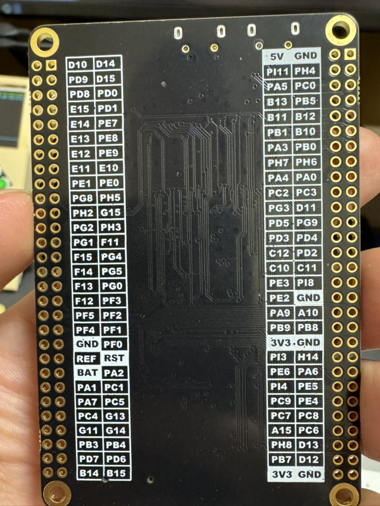
The core board has two double-row headers of 2 x 29 pins. The labels below are as printed on the back silkscreen. Some are shortened: D10 = PD10, E15 = PE15, G15 = PG15, F11 = PF11, B13 = PB13, C12 = PC12, A10 = PA10, H14 = PH14, A15 = PA15.
- L / R = left / right block as seen on the back silkscreen. Seen from the component side, the blocks swap sides.
- Position 1–29 counts from the end with
D10 D14/5V GND(the USB/SWD end of the board). - Line 1 / line 2 = first / second label column. Which physical hole row is which: check with a continuity tester once.
Left block (L)
| Pos | Line 1 label | Line 1 use | Line 2 label | Line 2 use |
|---|---|---|---|---|
| 1 | D10 |
SDRAM | D14 |
SDRAM |
| 2 | PD9 |
SDRAM | D15 |
SDRAM |
| 3 | PD8 |
SDRAM | PD0 |
SDRAM |
| 4 | E15 |
SDRAM | PD1 |
SDRAM |
| 5 | E14 |
SDRAM | PE7 |
SDRAM |
| 6 | E13 |
SDRAM | PE8 |
SDRAM |
| 7 | E12 |
SDRAM | PE9 |
SDRAM |
| 8 | E11 |
SDRAM | E10 |
SDRAM |
| 9 | PE1 |
SDRAM | PE0 |
SDRAM |
| 10 | PG8 |
SDRAM | PH5 |
SDRAM |
| 11 | PH2 |
SDRAM | G15 |
SDRAM |
| 12 | PG2 |
SDRAM | PH3 |
SDRAM |
| 13 | PG1 |
SDRAM | F11 |
SDRAM |
| 14 | F15 |
SDRAM | PG4 |
SDRAM |
| 15 | F14 |
SDRAM | PG5 |
SDRAM |
| 16 | F13 |
SDRAM | PG0 |
SDRAM |
| 17 | F12 |
SDRAM | PF3 |
SDRAM |
| 18 | PF5 |
SDRAM | PF2 |
SDRAM |
| 19 | PF4 |
SDRAM | PF1 |
SDRAM |
| 20 | GND |
GND | PF0 |
SDRAM |
| 21 | REF |
VREF+ | RST |
NRST |
| 22 | BAT |
VBAT | PA2 |
stick R-X |
| 23 | PA1 |
free | PC1 |
stick L-X |
| 24 | PA7 |
stick R-Y | PC5 |
free |
| 25 | PC4 |
stick L-Y | G13 |
free |
| 26 | G11 |
free | G14 |
free |
| 27 | PB3 |
SD D2 | PB4 |
SD D3 |
| 28 | PD7 |
SD CMD | PD6 |
SD CK |
| 29 | B14 |
SD D0 | B15 |
SD D1 |
Positions 1–20 and 27–29 are the on-board SDRAM and SD card. Connect nothing to them.
Right block (R)
| Pos | Line 1 label | Line 1 use | Line 2 label | Line 2 use |
|---|---|---|---|---|
| 1 | 5V |
5 V | GND |
GND |
| 2 | PI11 |
LTDC G6 | PH4 |
LTDC G4 |
| 3 | PA5 |
DAC R | PC0 |
LTDC R5 |
| 4 | B13 |
free | PB5 |
(unused, do not connect) |
| 5 | B11 |
free | B12 |
free |
| 6 | PB1 |
LTDC R6 | B10 |
free |
| 7 | PA3 |
LTDC B5 | PB0 |
LTDC R3 |
| 8 | PH7 |
free | PH6 |
btn RIGHT |
| 9 | PA4 |
DAC L | PA0 |
btn MENU |
| 10 | PC2 |
VS1003B MISO | PC3 |
VS1003B MOSI |
| 11 | PG3 |
free | D11 |
free |
| 12 | PD5 |
panel DISP | PG9 |
(unused, do not connect) |
| 13 | PD3 |
LTDC G7 | PD4 |
ESP32 DRDY |
| 14 | C12 |
free | PD2 |
ESP32 CS |
| 15 | C10 |
free | C11 |
free |
| 16 | PE3 |
free | PI8 |
VS1003B DREQ |
| 17 | PE2 |
ESP32 SCK | GND |
GND |
| 18 | PA9 |
USB VBUS sense | A10 |
LTDC B1 (not wired) |
| 19 | PB9 |
LTDC B7 | PB8 |
LTDC B6 |
| 20 | 3V3 |
3.3 V | GND |
GND |
| 21 | PI3 |
VS1003B XCS | H14 |
free |
| 22 | PE6 |
ESP32 MOSI | PA6 |
LTDC G2 |
| 23 | PI4 |
VS1003B XDCS | PE5 |
ESP32 MISO |
| 24 | PC9 |
LTDC G3 | PE4 |
5 V rail EN |
| 25 | PC7 |
free | PC8 |
free |
| 26 | A15 |
free | PC6 |
LTDC HSYNC |
| 27 | PH8 |
free | D13 |
free |
| 28 | PB7 |
free | D12 |
free |
| 29 | 3V3 |
3.3 V | GND |
GND |
Power and special pins
| Location | Label | Meaning |
|---|---|---|
| R1.1 | 5V |
5 V of the core board. Boost #2 feeds the board through this pin or through the USB jack: TBD |
| R1.2, R17.2, R20.2, R29.2, L20.1 | GND |
ground |
| R20.1, R29.1 | 3V3 |
3.3 V from the on-board regulator (panel logic, sticks, buttons) |
| L21.1 | REF |
VREF+ (ADC/DAC reference) |
| L21.2 | RST |
NRST. The mainboard's hard reset button shorts it to GND |
| L22.1 | BAT |
MCU VBAT; the battery is measured here. Limit 3.6 V; a full cell is 4.2 V. Never connect the cell straight to it; the circuit in between is TBD, see power.md |
The display lines CLK, VSYNC, DE, R4, R7, G5, B3, B4, the buttons PH9–PH12, PI5, PI6, PI7, PI10, and PI1/PI2 come out only on the "LCD interface" connector (see below).
Display ribbon (40-pin, folded)
The panel reaches the core board's 40-pin "LCD interface" connector through two FFC adapters and a 40-pin ribbon. Under each adapter the ribbon is folded in half, and each fold reverses the pin order (n ↔ 41 − n).
 display FPC  ──►  screen-side adapter  ──►  40-pin ribbon  ──►  board-side adapter  ──►  core board
 pin n             (fold #1, mirrored)       conductor k          (fold #2, mirrored)        "LCD interface" pin m
 (datasheet)       pad = 41 − n              (cable side)         m = 41 − k                 (as printed) + headers
The board-side adapter is a breakout point: the buttons and the LCD-only lines are taken from its pads. The screen-side adapter is wired by function from those pads and the header wires, using the panel table. The pad number is not the panel pin (for example VSYNC is on pad 32 but panel pin 33).
Board-side adapter pads:
| Pad (cable side) | FPC pin (board side) | STM32 | Signal |
|---|---|---|---|
| 40 | 1 | PE2 | ESP32 SPI4 SCK: leave the pad unconnected |
| 39 | 2 | PE3 | free |
| 38 | 3 | PD12 | free (planned vibration) |
| 36 | 5 | PD13 | free (planned LED) |
| 35 | 6 | PH7 | free |
| 34 | 7 | PH6 | button RIGHT |
| 33 | 8 | PF10 | LTDC DE |
| 32 | 9 | PI9 | LTDC VSYNC |
| 31 | 10 | PI10 | button UP |
| 30 | 11 | PG7 | LTDC CLK |
| 29 | 12 | — | not connected |
| 28 | 13 | PI7 | button LEFT |
| 27 | 14 | PI6 | button DOWN |
| 26 | 15 | PI5 | button SELECT |
| 25 | 16 | PG12 | LTDC B4 |
| 24 | 17 | PA8 | LTDC B3 |
| 19 | 22 | PI2 | VS1003B XRST (planned) |
| 18 | 23 | PI1 | VS1003B SCK (planned) |
| 17 | 24 | PI0 | LTDC G5 |
| 16 | 25 | PH15 | LTDC R4 |
| 15 | 26 | PG10 | free |
| 14 | 27 | PH13 | free |
| 11 | 30 | 3V3 | 3.3 V |
| 10 | 31 | PG6 | LTDC R7 |
| 9 | 32 | PH12 | button Y |
| 8 | 33 | PH11 | button X |
| 7 | 34 | PH10 | button B |
| 6 | 35 | PH9 | button A |
FPC pins 4, 18–21, 28 and 36–40 are not documented (TBD).
Continuity check (power off, battery unplugged):
- Set the meter to continuity. Put one probe on the STM32 signal: the header pin or the board-side adapter pad.
- Slide the other probe along the panel FPC contacts (or the screen-side adapter pads; pad = 41 − panel pin) until it beeps.
- Note the panel pin for CLK, HSYNC, VSYNC, DE, DISP and every R/G/B line. Correct any line that does not match the table below.
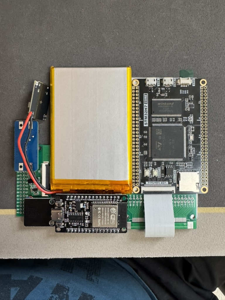
Top view of the reference unit: STM32H7 CORE board (Winbond SDRAM, USB and UART micro-USB, SWD connector, RESET/BOOT0 buttons, microSD slot, "LCD interface" FPC), the Li-Po pack, the ESP32 DevKit, the boost modules, and the green 40-pin FFC adapters with the grey ribbon.
Panel FPC pinout (HL043PQIPS-500)
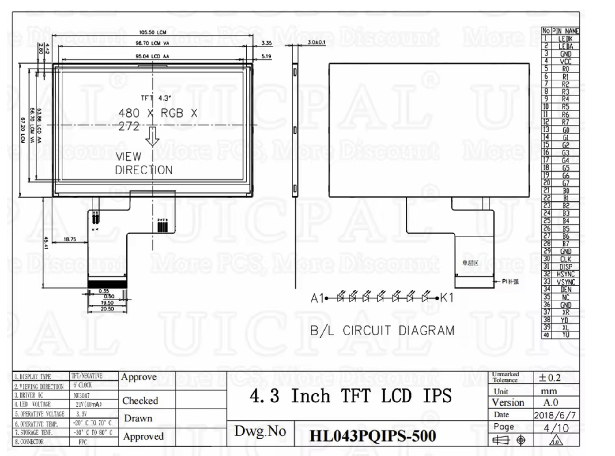
HL043PQIPS-500: 4.3" TFT IPS, 480 x RGB x 272, driver IC NV3047, logic 3.3 V, backlight 21 V / 40 mA (8 LEDs in series), 40-pin FPC with 0.5 mm pitch, active area 95.04 x 53.86 mm, outline 105.5 x 67.2 mm, operating −20…70 °C, storage −30…80 °C.
| Panel pin | Name | Connect to | Pick it up at | Screen-side adapter pad (41 − pin) |
|---|---|---|---|---|
| 1 | LEDK | 21 V booster − | booster output | 40 |
| 2 | LEDA | 21 V booster + | booster output | 39 |
| 3 | GND | GND | 38 | |
| 4 | VCC | 3.3 V | R20.1 / R29.1, or pad 11 | 37 |
| 5–7 | R0–R2 | GND (recommendation) | 36–34 | |
| 8 | R3 | PB0 | R7.2 | 33 |
| 9 | R4 | PH15 | pad 16 | 32 |
| 10 | R5 | PC0 | R3.2 | 31 |
| 11 | R6 | PB1 | R6.1 | 30 |
| 12 | R7 | PG6 | pad 10 | 29 |
| 13–14 | G0–G1 | GND (recommendation) | 28–27 | |
| 15 | G2 | PA6 | R22.2 | 26 |
| 16 | G3 | PC9 | R24.1 | 25 |
| 17 | G4 | PH4 | R2.2 | 24 |
| 18 | G5 | PI0 | pad 17 | 23 |
| 19 | G6 | PI11 | R2.1 | 22 |
| 20 | G7 | PD3 | R13.1 | 21 |
| 21–23 | B0–B2 | GND (recommendation) | 20–18 | |
| 24 | B3 | PA8 | pad 24 | 17 |
| 25 | B4 | PG12 | pad 25 | 16 |
| 26 | B5 | PA3 | R7.1 | 15 |
| 27 | B6 | PB8 | R19.2 | 14 |
| 28 | B7 | PB9 | R19.1 | 13 |
| 29 | GND | GND | 12 | |
| 30 | CLK | PG7 via 33 Ω | pad 30 | 11 |
| 31 | DISP | PD5 | R12.1 | 10 |
| 32 | HSYNC | PC6 via 33 Ω | R26.2 | 9 |
| 33 | VSYNC | PI9 via 33 Ω | pad 32 | 8 |
| 34 | DEN (data enable) | PF10 via 33 Ω | pad 33 | 7 |
| 35 | NC | — | 6 | |
| 36 | GND | GND | 5 | |
| 37–40 | XR, YD, XL, YU (resistive touch) | not connected | 4–1 |
ESP32 DevKit pins
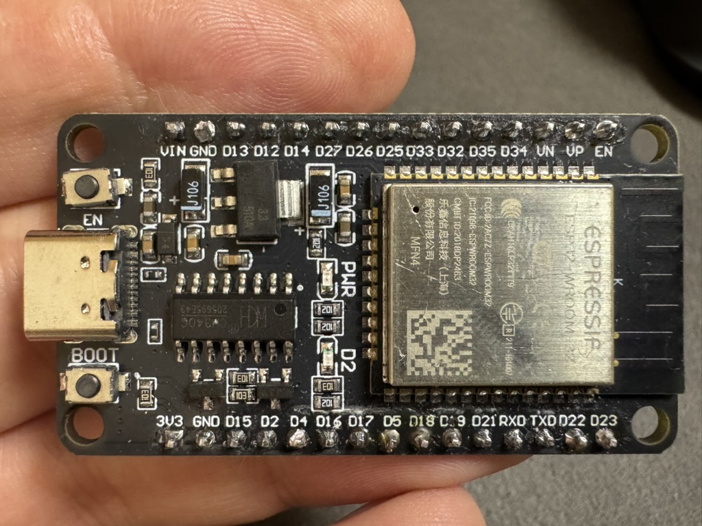
ESP32-WROOM-32 DevKit with CH340 USB-UART, USB-C and EN/BOOT buttons. Top row: VIN GND D13 D12 D14 D27 D26 D25 D33 D32 D35 D34 VN VP EN. Bottom row: 3V3 GND D15 D2 D4 D16 D17 D5 D18 D19 D21 RXD TXD D22 D23.
| DevKit label | ESP32 GPIO | Function | Direction |
|---|---|---|---|
| D18 | GPIO18 | SPI SCLK | in |
| D23 | GPIO23 | SPI MOSI | in |
| D19 | GPIO19 | SPI MISO | out |
| D5 | GPIO5 | SPI CS; strapping pin, ~10 kΩ pull-up to 3.3 V | in |
| D4 | GPIO4 | DRDY, starts LOW | out |
| TXD / RXD | GPIO1 / GPIO3 | log console, 115200 baud, via the DevKit USB | — |
| VIN | — | +5 V from boost #1 (PE4 rail) | — |
| GND | — | ground | — |
Audio amplifier (HW-301 PAM8406)
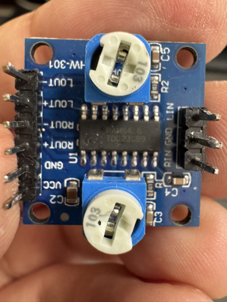
| From | To | Notes |
|---|---|---|
| PA4, R9.1 | LIN |
|
| PA5, R3.1 | RIN |
|
| core-board GND | input GND |
keep it separate from the speaker leads |
| boost #1 output (PE4 rail) | VCC / GND |
through the LC filter |
LOUT+ / LOUT- |
left speaker | bridge-tied: never connect LOUT-/ROUT- to GND |
ROUT+ / ROUT- |
right speaker | 20 mm speakers (see bom.md) |
Power wiring: power.md.