Core8Bit power
Power rails, battery, wiring and the firmware power thresholds.
Safety. Solder only with the battery disconnected. Check polarity twice. Never short 5 V to 3.3 V. Do not use a damaged or swollen cell.
Contents
- Rails
- PE4: the switched 5 V rail
- Battery
- How the battery is measured
- Power policy
- Charging detection
- Wiring
- Mainboard plan: single USB-C and hard reset
- Known issues
Rails
| Rail | Made by | Feeds | Switched by |
|---|---|---|---|
| VBAT_CELL (3.0–4.2 V) | Li-Po 606090 1S through the charger / "battery driver" board | boost #1 and boost #2 inputs | — |
| 5 V permanent | boost #2 (step-up module) | STM32 core board | always on |
| 3.3 V | regulator on the core board | MCU, SDRAM, QSPI, SD card, panel logic, sticks, buttons; header 3V3 (R20.1, R29.1) |
— |
| 5 V switched | boost #1 (step-up module) | ESP32 VIN, PAM8406 VCC, 21 V backlight booster | PE4: HIGH = on, LOW = off |
| ~21 V backlight | 21 V booster, fed from boost #1 | panel backlight (21 V / 40 mA) | follows PE4 |
| USB 5 V | USB cable | charger input | — |
Do not use boost #2 EN as a reset or power switch. With EN LOW a plain asynchronous boost still passes about VBAT − 0.3 V to its output, so the core board stays powered. The hard reset shorts NRST to GND instead (see Mainboard plan).
PE4: the switched 5 V rail
| Moment | PE4 |
|---|---|
| Reset | LOW. Fit a 100 kΩ pull-down from boost #1 EN to GND so the rail stays off while the MCU is in reset |
| Cold-boot battery check | LOW; the cell is measured unloaded |
| Audio start | the DAC ramps to mid-scale first, then PE4 goes HIGH, so the amplifier does not pop |
| Backlight on | DISP (PD5) HIGH → PE4 HIGH → picture |
| Sleep / shutdown | picture off → DISP LOW → PE4 LOW → 200 ms → audio off |
PE4 also feeds the ESP32 and the amplifier. Turning the backlight off turns them off too.
Battery
| Item | Value |
|---|---|
| Cell | Li-Po 606090, 1S, 3800 mAh (4000 mAh is better), with a protection board (BMS) |
| Charger | charger / "battery driver" board (see bom.md) |
| Fuel gauge | none; the firmware measures voltage only |
How the battery is measured
- The firmware reads the MCU VBAT pin (core-board header
BAT, L22.1) through the MCU's internal /4 divider, referenced to the internal VREFINT. - It subtracts a fixed 250 mV offset for the drop between the cell and the VBAT pin.
- The VBAT pin is rated for 3.6 V maximum; a full cell is 4.2 V. Do not connect the cell straight to
BAT. The circuit between the cell andBATis TBD.
Power policy
| Situation | Threshold | Behaviour |
|---|---|---|
| Cold boot | 10 % | below 10 % the console stays dark and measures again every 20 s, on a MENU press, or when the charger is plugged in |
| Wi-Fi | 15 % | below 15 % the ESP32 sleeps; it comes back by itself when the charge recovers |
| Low warning | 10 % | 5 s banner and a red battery icon |
| Blink | 5 % | the battery icon blinks |
| Auto-sleep | 5 %, or 3050 mV, held for 5 s | the console sleeps. Never while charging |
| Wake from sleep | 6 % | below 6 % the console does not wake |
0 % = 3050 mV. The cold-boot check is there because starting the 5 V rail on a flat cell trips the cell's BMS.
Charging detection
- On the wired build PA9 follows the 5 V rail and is not used. The firmware detects charging from a voltage rise of ≥ 180 mV over about 12 s.
- On the mainboard PA9 measures the USB-C VBUS through a divider, see mainboard.md. In OTG mode PA9 also sees 5 V. The microphone moves from PA9 to another free ADC input (TBD).
Wiring
USB (charge) ─► charger / "battery driver" board ◄─► Li-Po 606090 1S
                          │ OUT+
                          ├─► boost #2 (always on) ─► 5 V ─► core board (5V pin or USB: TBD) ─► on-board 3.3 V
                          │                                     └─ 3V3 headers: panel logic, sticks, buttons
                          └─► boost #1 (EN ◄─ PE4, header R24.2) ─► 5 V switched ─┬─► ESP32 DevKit VIN
                                                                                 ├─► PAM8406 VCC
                                                                                 └─► 21 V booster ─► panel backlight
core-board header BAT (L22.1) = MCU VBAT (max 3.6 V)
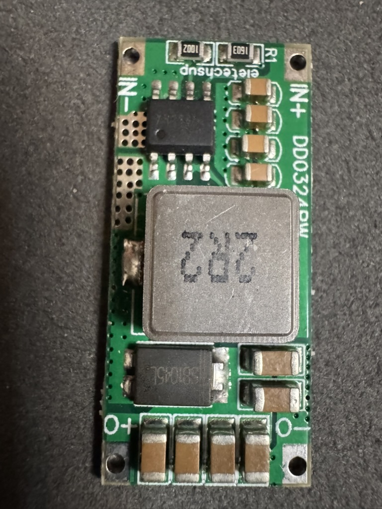
| From | To | Notes |
|---|---|---|
| Li-Po + / − | charger board battery pads | check polarity twice |
| charger OUT+ / − | boost #1 IN+/IN−, boost #2 IN+/IN− | 22–24 AWG, from one point (star) |
| boost #2 O+ / O− | core board 5 V / GND | always on |
| STM32 PE4 (R24.2) | boost #1 EN | active HIGH; 100 kΩ pull-down to GND. The module has no labelled EN pad: use the EN/SHDN pin of its SO-8 controller |
| boost #1 O+ / O− | ESP32 VIN/GND, PAM8406 VCC/GND, 21 V booster input | 22–24 AWG |
| GND | common star point |
Mainboard plan: single USB-C and hard reset
In development (mainboard.md). The wired build does not have this. Values and pins are TBD.
USB-C VBUS ─┬─► SS34 / ideal diode (P-MOSFET) ─► charger board input ◄─► Li-Po 606090 1S
            │                                      │ CE ◄─ charging off during OTG (TBD)
            ├─► divider ─► PA9 (VBUS sense)        ├─► boost #2 ─► STM32 (NRST ◄─ reset button → GND)
            │                                      └─► boost #1 (EN ◄─ PE4) ─► ESP32, PAM8406, 21 V
            └─◄─ P-MOSFET switch ◄─ 5 V of boost #1 (PE4)
                     ▲ OTG_EN (GPIO, TBD)
CC1/CC2 ─► TUSB320 (DRP) ─► INT/ID ─► GPIO (TBD)
| Block | Design |
|---|---|
| Charging input | VBUS → SS34 (Schottky) or P-MOSFET ideal diode → charger board input. Stops 5 V flowing back into the connector |
| OTG power | P-MOSFET switch from the boost #1 5 V rail to VBUS, driven by a GPIO. Works only while PE4 = HIGH |
| Charge disable | the charger's CE is off during OTG, so the battery does not charge from its own boost |
| CC | TUSB320 in DRP mode; INT/ID output to a GPIO. Do not use fixed 5.1 kΩ (sink-only) or 56 kΩ (host-only) resistors |
| VBUS sense | PA9 through a divider |
| Hard reset | SMD micro button on the back, under a paperclip hole in case-back. It shorts the core board's NRST (RST) pin to GND, with a 100 nF capacitor to GND against bounce. Releasing it restarts the STM32 |
PE4 LOW does not fully unpower the 5 V loads with a plain asynchronous boost (VBAT − 0.3 V passes through). For a full cut-off use a boost with load disconnect or a switch on its output.
Known issues
| Symptom | Cause | Fix |
|---|---|---|
| Amplifier pop at reset | PE4 floats HIGH during reset | 100 kΩ pull-down on boost #1 EN |
| Console reboots at start-up on a flat battery | 5 V inrush trips the cell's BMS | charge the battery; cold boot needs 10 % |
| Charging icon unreliable | PA9 follows the 5 V rail | expected on the wired build; charging is detected from the voltage rise |