Core8Bit hardware
Core8Bit is a DIY handheld game console built from off-the-shelf modules: an STM32H7 core board, a 4.3" 480 x 272 IPS panel, an ESP32 for Wi-Fi, two analog sticks, ten buttons, a stereo amplifier and a single-cell Li-Po battery. This page is the specification. For wiring see pinout.md, for power power.md, for parts bom.md, for the build assembly.md. The mainboard that replaces the wiring is described in mainboard.md (in development).
Contents#
Block diagram#
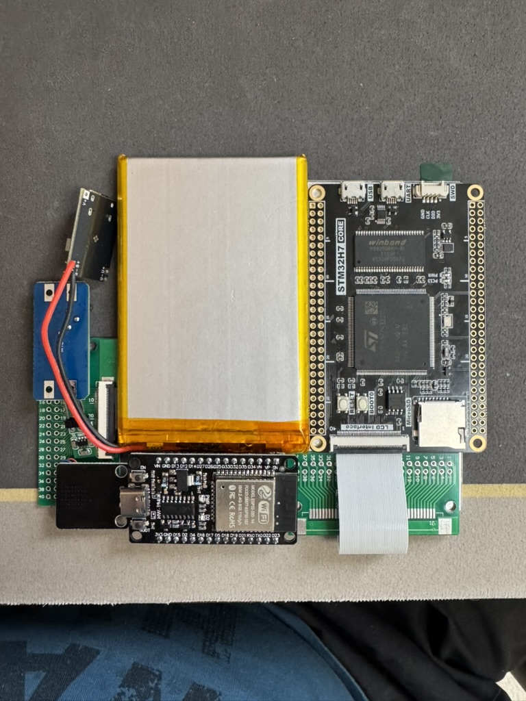
 USB ─► charger / "battery driver" ◄─► Li-Po 606090 1S (3800–4000 mAh)
              │
              ├─► boost #2 (always on) ─► 5 V ─► STM32H7 CORE board (on-board 3.3 V)
              └─► boost #1 (EN = PE4) ─► 5 V switched ─┬─► ESP32 DevKit (VIN)
                                                      ├─► PAM8406 amplifier ─► 2 speakers
                                                      └─► 21 V booster ─► panel backlight

  STM32H7 CORE board (480 MHz)
   |-- FMC  ------- 32 MB SDRAM (Winbond W9825G6KH, on board)
   |-- QUADSPI ---- 16 MB NOR flash (W25Q128)
   |-- SDMMC2 ----- microSD slot (on board), 4-bit
   |-- LTDC ------- "LCD interface" FPC + headers ─► 2 folded FFC adapters ─► HL043PQIPS-500 4.3" IPS
   |-- DAC1 ------- PA4/PA5 ─► PAM8406 LIN/RIN
   |-- ADC2 ------- 2 analog sticks (4 axes)
   |-- GPIO ------- 10 buttons (active HIGH)
   |-- SPI4 ------- ESP32 (SPI slave) + CS + DRDY
   |-- SPI2 ------- VS1003B MP3 decoder (planned for the mainboard)
   |-- USB OTG FS - on-board micro-USB: SD card mode / debug
   '-- SWD ------- on-board SWD connector (ST-Link)
Main MCU#
| Item |
Value |
| Part |
STM32H753IIT6 or STM32H743IIT6 |
| Package |
LQFP176. The LQFP100 "VIT6" version does not work: it has no ports H and I |
| Core |
Cortex-M7, 480 MHz, hardware double-precision FPU |
| On-chip flash |
2 MB |
| Internal SRAM |
DTCM 128 KB, AXI 512 KB, D2 288 KB, D3 64 KB, ITCM 64 KB |
| Crystals |
HSE 25 MHz, LSE 32.768 kHz (both on the core board) |
Memories#
| Memory |
Part |
Size |
Interface |
| SDRAM |
W9825G6KH (Winbond) |
32 MB |
FMC bank 1, 16-bit, 120 MHz |
| NOR flash |
W25Q128 (JV or compatible) |
16 MB |
QUADSPI bank 1, 50 MHz. Holds the sound bank at 0x90010000 |
| microSD |
card slot on the core board |
64 GB recommended |
SDMMC2, 4-bit, 40 MHz (high-speed card needed). FAT32 or exFAT |
Display#
| Item |
Value |
| Panel |
HL043PQIPS-500, 4.3" TFT IPS, 500 nit, 480 x RGB x 272, driver NV3047, 3.3 V logic, 40-pin 0.5 mm FPC, active area 95.04 x 53.86 mm |
| Format |
480 x 272, RGB565 on the high bits (R3–R7, G2–G7, B3–B7); the low panel bits are not used |
| Timing |
parallel RGB with DE, 12.5 MHz pixel clock, about 87 Hz. HSYNC/VSYNC active low, DE active high. HSW 11 / HBP 10 / HFP 10, VSW 3 / VBP 2 / VFP 2 |
| Panel enable |
PD5 → panel DISP (pin 31), HIGH = on |
| Backlight |
8 LEDs in series, 21 V / 40 mA, from the 21 V booster on the PE4 rail. On/off only, no dimming |
| Wiring |
"LCD interface" FPC + header wires, through two folded 40-pin FFC adapters, see pinout.md |
Switch-on order: DISP (PD5) HIGH, then PE4 HIGH, then the picture. Switch-off is the reverse.
Audio#
| Item |
Value |
| Output |
on-chip DAC1, 12-bit stereo: PA4 = left, PA5 = right |
| Sample rate |
22 050 Hz |
| Amplifier |
PAM8406 (HW-301 board) with two 10 kΩ volume trimmers, powered from the PE4 rail. Bridge-tied outputs to two 20 mm speakers in the case's speaker enclosures |
| Pop suppression |
the firmware holds PE4 LOW at reset and ramps the DAC to mid-scale before it switches the rail on |
| MP3 decoder |
VS1003B on SPI2, planned for the mainboard. Volume over SPI (SCI_VOL). Its line output is mixed with the DAC through ~1 µF + ~10 kΩ per source into the PAM8406 inputs, see mainboard.md |
Ten buttons, all active HIGH: a press connects the pin to 3.3 V. The internal pull-downs are on.
| Button |
Pin |
Role |
| UP / DOWN / LEFT / RIGHT |
PI10 / PI6 / PI7 / PH6 |
D-pad |
| A / B / X / Y |
PH9 / PH10 / PH11 / PH12 |
face buttons |
| MENU |
PA0 |
combo modifier: MENU+A console, MENU+B exit game, MENU+UP Wi-Fi, MENU+DOWN sleep, MENU+LEFT/RIGHT volume. Also wakes the console |
| SELECT |
PI5 |
opens and closes the system menu |
There are no shoulder buttons and no stick-click buttons.
Analog sticks#
| Stick / axis |
Pin |
ADC channel |
| Right X |
PA2 |
ADC2_INP14 |
| Right Y |
PA7 |
ADC2_INP7 |
| Left X |
PC1 |
ADC2_INP11 |
| Left Y |
PC4 |
ADC2_INP4 |
- Each axis is a potentiometer between 3.3 V and GND, with the wiper on the ADC pin.
- Calibrate every new build in SELECT → Settings → Sticks: centre, direction, rotate, release. The wizard detects inverted axes. The result is saved in
0:/System/joystick_cal.dat.
Wi-Fi co-processor (ESP32)#
| Item |
Value |
| Module |
ESP32-WROOM-32 (classic ESP32, not S2/S3/C3) on a DevKit with CH340 and USB-C; at least 2 MB flash |
| Link |
STM32 SPI4 master ↔ ESP32 SPI slave, mode 0, 7.5 MHz, 256-byte packets |
| Handshake |
CS = PD2 → GPIO5 (active LOW). DRDY = GPIO4 → PD4 (HIGH = data ready) |
| Reset |
the ESP32 resets only when the PE4 rail cycles or with its own EN button |
| Power |
DevKit VIN from boost #1 (PE4 rail) |
| Log console |
UART0, 115200 baud, on the DevKit USB |
When it is online the Wi-Fi module also sends anonymous usage statistics; see telemetry.md for what is sent and how to turn it off.
USB#
| Item |
Value |
| Port |
on-board micro-USB "USB": USB FS device, PA11 = D−, PA12 = D+ |
| SD card mode |
the PC sees "Core8Bit MSC" (the SD card). Start it from SELECT → Settings → SD card |
| Debug |
"Core8Bit Debug CDC" serial port |
| VBUS |
PA9. On the wired build it follows the 5 V rail, so charging is detected from the battery voltage instead |
| Mainboard plan |
one external USB-C for charging, PC and OTG, see mainboard.md |
Debug (SWD)#
- Flash and debug over SWD (PA13 SWDIO, PA14 SWCLK) with an ST-Link on the core board's "SWD" connector.
- SWO trace and 4-wire JTAG are not available: PB3 and PB4 are used by the SD card.
Power (summary)#
- Battery: Li-Po 606090 1S, 3800 mAh (4000 mAh is better), through the charger / "battery driver" board.
- Boost #2 (always on) feeds the core board; its on-board regulator makes 3.3 V.
- Boost #1, enabled by PE4 (HIGH = on), feeds the ESP32, the PAM8406 and the 21 V backlight booster.
- The battery is measured on the MCU VBAT input (header
BAT).
- Thresholds: cold boot from 10 %, Wi-Fi off below 15 %, sleep below 5 %, wake from 6 %.
- Mainboard plan: one USB-C port (charging + OTG) and a hard reset button that shorts the core board's NRST to GND, see power.md.
Details: power.md.
Case#
- Body: 3D printed, with speaker enclosures for 20 mm speakers.
- Faceplate: laser cut.
- Hardware: display cover glass, soft rubber button caps, 18 mm screws, 14 mm standoffs (bom.md).
- Files: the STL for case + speaker enclosures will be sold on itch.io; case-only files as an optional donation.
- Printing and assembly: assembly.md. For the mainboard,
case-back.stl gets a paperclip hole and channel for the hard reset button, see mainboard.md.